Transistors#
Transistors are the single most important component for digital electronics because they are able to act as independent switches. There are several types of transistors, but we will focus on Bipolar Junction Transistors (BJTs), which are essentially a semiconductor sandwich. There are thus two types of BJTs: NPN and PNP.
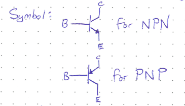
Our discussion will focus on the NPN BJT, but the concepts are the same for PNP transistors, simply replacing negative charge carriers with positive ones.
NPN Transistor#
A BJT has three terminals known as base, emitter, and collector. The base section is in the middle, and is very thin and only lightly doped so that there is only one hole for every hundred donor electrons in the emitter N-type section.
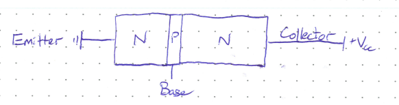
It may seem that this sandwich structure would not be very useful since the emitter-base (EB) junction forms a diode facing one way, and the collector-base (CB) junction a diode facing the other direction, thus making it seem as if no current can flow at all due to the one way nature of diodes. However, interesting things happen by including the base terminal in the middle.
If the BE junction is forward biased, electrons will flow out of the emitter and into the base and circulate in that loop. As mentioned above though, the base is very thin, and the emitter is very heavily doped with free electrons relative to the base. The rush of free electrons into the base leads to some spilling over into the collector and being attracted to the positive terminal there. You can think of this as the electrons momentum carrying them across the depletion region barrier, but the truth involves more quantum mechanics than I am willing to get into.
Now, because of the mismatch in doping and the thin base, a small amount of current from base to emitter leads to a LARGE current from collector to emitter. This amplification was one of the first primary uses of transistors, and is still used today in devices like hearing aids. When in amplification mode, the current through the collector (\(I_C\)) is larger than the current through the base terminal (\(I_B\)) by a constant factor, called the gain (\(\beta\)).
Depending on the exact setup of the circuit, \(\beta\) typically ranges between 100 and 300. However, there is a limit to how much current can actually go through the CE path. We cannot amplify things indefinitely. As we approach this limit, \(\beta\) becomes small, and we say the transistor is saturated. Consider the following diagram where the points \(B, C\), and \(E\) show the Base, Collector and Emitter respectively:
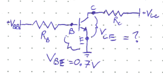
Although the potential drop across the BE junction is 0.7 V, the voltage drop from C to E is variable and changes as the BE current modifies the depletion regions inside the transistor.
Concept Check:
Why is the potential drop across the BE junction 0.7 V?
Solution
The BE junction is essentially a standard diode (P type semiconductor on one side, N-type on the other). Standard silicon diodes have a threshold voltage of \(V_\gamma = 0.7\) V. This threshold voltage is essentially always the potential drop across a diode with current flowing through it. If there was less, then current couldn’t flow at all. If there was a higher potential difference, then the current would increase until the potential lost across \(R_B\) (from Ohm’s Law) led to \(V_B\) bottoming out at the minimum 0.7 V.
For digital electronics, we don’t want amplification. We want discrete ON/OFF states. We want switches, all or nothing, 0 or 1. We want the transistor to be saturated and \(I_C\) to be at a maximum. In this case, what is \(V_{CE}\)? Let’s use KVL to explore how \(I_C\) changes with \(V_{CE}\), and see when the current is at a maximum. From KVL going down the right path:
Rearranging this equation yields:
A plot of this relationship is linear with a negative slope and a positive intercept. Recalling that \(V_{CE}\) cannot be negative because of how we have wired the circuit, that means the maximum current occurs when \(V_{CE} = 0\). When a transistor is saturated, current can flow through the CE path as if it offered no resistance and was the same as a wire. In reality, no transistor is perfect and there will be some small voltage drop from C to E in the range of 0.05 to 0.3 V.
Transistor Modes#
To summarize, a transistor can be in one of four states:
- Cut Off
When the voltage at the base is smaller than that of the emitter (\(V_B \leq\ V_E\)) and the collector (\(V_B \leq\ V_C\)), then no current can flow through the base at all. And thus no current can flow the the CE path of the transistor either. No current can flow at all and the transistor is in the OFF state when thinking digitally.
- Amplification
When the voltage at the base is greater than that of the emitter, but smaller than the collector (\(V_E < V_B < V _C\)), a small current will flow through the BE junction, triggering a much, much larger current to flow through the CE path. Gain values (\(\beta\)) are approximately 100 or greater. There will still be a significant potential difference between collector and emitter.
- Saturation
Current flows through the BE junction, but the current flowing down the CE path is reaching its maximum. This means that the potential drop from collector to emitter is almost zero (\(V_E < V_B\) and \(V_C < V_B\)). Gain values will be on the order of around 10. In the digital context, this transistor is in the ON state.
- Reverse Amplification
Alright, we haven’t talked about this, but you can wire a transistor incorrectly. The NPN sandwich looks symmetric, but it really is not. The doping levels are different in the collector and emitter. The transistor is designed for current to flow from base to emitter, but you can get it to flow from base to collector (\(V_C < V_B < V _E\)). An amplified current would then flow from the emitter to the collector, in the opposite direction from what is intended. This is generally bad and can damage your transistor.
An interactive demo to play with these scenarios can be found here. First try flipping the switch open and closed to see how removing the applied voltage at the base affects the CE current. Then, play with the resistance value of the top resistor to try to bring the transistor from amplification mode to saturation mode. Pay particular attention to what happens to the voltage at the collector terminal of the transistor.
Ensuring Saturation#
Since saturation is so important to digital electronics, how do we ensure saturation? It is actually not trivial. Typically, we would first use a resistor value to make sure that enough current can run through the CE path to power whatever function is desired (e.g. turn a light bulb on). Once that is known, use a restor to set the BE current to be some fraction of that. An arbitrary fraction of 1/10 is usually used, making \(\beta = 10\). Recall that typical gains in amplification are around 100, so anything much smaller than that is guaranteed to be close to saturation. Finally we confirm that the transistor is saturated with the following process:
Assume saturation, i.e. assume \(V_{CE} = 0\).
Determine \(I_B\) using Kirchoff’s Laws.
Determine \(I_C\) using Kirchoff’s Laws.
Confirm that \(\beta\) is small, and thus our initial assumption of saturation was valid.
Example
Show that the following transistor is saturated. The threshold voltage of the LED is 1.8 V.
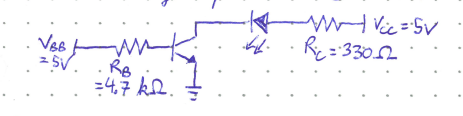
We start by assuming saturation and that \(V_{CE} = 0\). It is important that we confirm this assumption at the end.
Determine \(I_B\).
Using KVL: \(V_{BB} = I_BR_B + V_{BE}\).
Plugging in the given values of \(V_{BB} = 5\) V, \(R_B = 4700 \Omega\), and \(V_{BE} = 0.7\) V (because it is a junction diode) yields a value for \(I_B\) of
Determine \(I_C\)
Similarly as above, from KVL: \( V_{CC} = I_CR_C + V_{LED} + V_{CE} \).
Plugging in the values \(V_{CC} = 5\) V, \(R_C = 330 \Omega\), \(V_{LED} = 1.8\) V, and \(V_{CE} = 0\) V from our initial assumption, this yields
Determine \(\beta\).
\(\beta = \frac{I_C}{I_B} = 10.6\). This is much less than the gain expected from amplification mode, so we are indeed in saturation.